Then I stumbled on this FPGA Based Logic Analyzer. It's works on the still-available, $100 "S3BOARD", and the FPGA firmware is GPL. (It also has somewhat more memory than minila, and can also go up to 200MHz. On the other hand, it doesn't have a mode like minila's "state analysis", and it transfers over slow RS232 serial instead of EPP). I got the board today, and have some initial experiences to report.
I already had Xilinx Webpack installed from earlier work on mesa boards, so it wasn't hard to build the firmware, though it did confuse me for an hour how to program the so-called "platform flash" so that the board would boot in its logic analyzer personality. (the answer involves launching a program called "impact" to create the programming file for the flash, which is different from the programming file for the FPGA itself). Later on, I modified the constraints file to add internal pull-downs on the inputs; without that, the unused inputs worked as marvelous 120Hz antennas.
Later I had trouble getting the java-based GUI to work, because it could not find the serial communication library (and also wasn't compatible with gcj for some swing-related reason; I installed sun java instead). I ultimately found the answer, though I took the coward's way--copying files into the sun java installation area--instead of the method that alistair suggested one post further down. Like rscott13, I was just so relieved to have the software working at all.
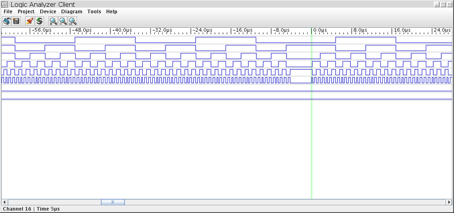
Besides the start-up problems, I've hit one small bug in the GUI: I selected only channel-group 0 and 200MHz sample rate. What I got was my desired signal interleaved with "0"s. When I selected groups 0 and 1, 200MHz sample rate worked. (so far any input signals I've tried have been at much more modest rates of under 5MHz)
The FPGA is not 5V tolerant and no protection is built into the board. The FPGA input pins do have protection diodes, though, so I designed a separate "input conditioning" board which simply consists of a 1.4K series resistor on each input signal. It also breaks the signals into the 4 groups of 8 and provides a ground for each group. This might allow something like .35mA of protection diode current per input, while the datasheet permits up to 100mA per input on up to 100 inputs (which I imagine has to be a mistake, or at least subject to other thermal limits). This simple method for 5V compatability seems to work so far.
When capturing traces of modest length (8k samples), the delay imposed by the serial link is tolerable. When getting a full 256k samples, though, you're looking more than a moment of time. My next modification may be to place a 1MB/s serial output on some unused pins--maybe the PS/2 connector--and run those through the USB-serial chip on an arduino board, which is supposed to work with rates up to 3Mb/s. (1MB/s is the fastest rate that is exactly obtainable by both devices) If that works i'll buy a dedicated TTL-serial-to-USB converter for the board.
Entry first conceived on 22 July 2008, 3:09 UTC, last modified on 15 January 2012, 3:46 UTC
Website Copyright © 2004-2024 Jeff Epler